Contents
Equipment/Parts Needed
- Quartus IIR Web Edition V9.1 SP2 software by Altera Corporation
- USB drive to save your files
Objective
- Learn how to create and modify a VHDL text file and symbol file
- Program the Altera’s DE2 FPGA board
Discussion
VHDL is a high-level, modular language first defined by the IEEE Std 1076-1987. This standard has been revised by IEEE Std 1076-1993 and again by IEEE Std 1076.3-1997. The V in the acronym VHDL represents Very High Speed Integrated Circuit (VHSIC) and HDL stands for Hardware Descriptive Language. Any text editor can be used to create VHDL Design Files (.vhd); however it is recommended to use the Quartus II Text Editor to take advantage of features unique to this editor, including syntax coloring of reserved words and comments, error detection, and VHDL templates.
From the Text Editor, a Block Symbol file (.bsf) is created (File – Create/Update – Create Symbol File For Current File) that can be included into any Block Design file (.bdf). Altera’s version of VHDL, (AHDL Include File.inc) can be created and placed into Text Design files (.tdf); however, this lab manual only focuses on VHDL files. VHDL Design files can contain any combination of primitives, megafunctions, macrofunctions, and user defined functions integrated into hierarchical projects.
By no means will you become an expert in writing VHDL files after completing the VHDL labs in this manual. VHDL is only introduced as a means to modularize hardware designs using software. The entire behavior of hardware circuits are encoded in software and due to the densities of today’s ASICs (Application Specific Integrated Circuits), FPGAs (Field Programmable Gate Arrays), and CPLDs (Complex Programmable Logic Devices), the only way to manipulate the hardware is through software. Students seeking Associate and Baccalaureate degrees should learn how to read, interpret, modify, compile, and verify basic VHDL design files.
New toolbar icons associated with the Text Editor are shown in Figure 7-1.
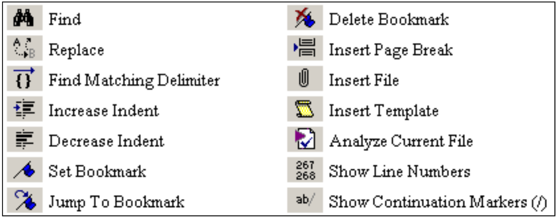
Figure 7-1: New toolbar icons associated with the Text Editor
Part 1 Procedure
Creating a New Project
- Open the Quartus II software. Select File – New Project Wizard. Enter the appropriate drive letter for the designated storage area on the computer you are using followed by the working directory C:\altera\91sp2\quartus\kwon\Lab7. You need to go through the step from 1 through 8 in the Part 1 of Lab6 manual. Don’t forget to create the folder Lab7 under the subfolder of your last name. Assign the project name Lab7_1 (Figure 7-2), assign Cyclone II for the device family, and select the EP2C35F672C6 chip in the Family & device settings [page of 3 of 5].
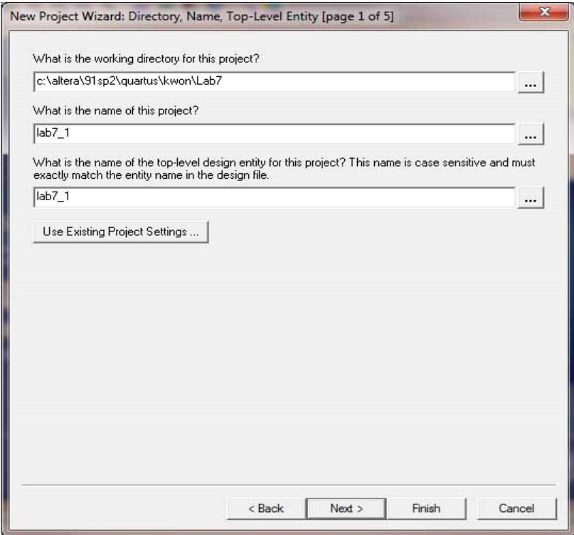
Figure 7-2
Creating a VHDL File (bdf)
- Open a new VHDL Device Design file (File > New) by highlighting VHDL File. And click OK. A Text Editor opens titled Vhdl1.vhd* with the first line numbered in light gray text. Type the VHDL code shown in Text Box 1. All reserved words will appear as blue text, comments are green, and all other characters will be black. Reserved words shown in Text Box 1 are in capital letters; however, VHDL is not case sensitive.
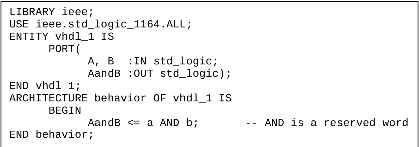
Text Box 1
- Save the VHDL file as vhdl_1.vhd as part of our project under your subfolder. Place a check mark in the space labeled Add file to current project and press Save (See Figure 7-3).
- Select File – Create/Update – Create Symbol Files for Current File to create a symbol file for the VHDL code entered. A Compilation Report window initially displays “Report not available”; however, be patient. A display window should soon appear stating that the Create Symbol File was (or not) successful. Click OK and close the Compilation Report window.
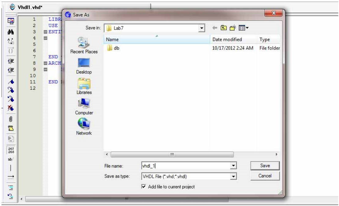
Figure 7-3
- The compiler should display the successful message. If you made typographical errors, the compiler messenger (see the Messages Utility Window at the bottom of the screen) will identify each error and pinpoint the line the error occurs on or near. Double-click on the (red) errors, starting with the first one on the list, and correct all typographical errors.
- Once the errors have been corrected, save the file (File – Save) and again try to create a default symbol. When you try to create a symbol for the second time, the software prompts you to overwrite the existing file. Click on OK to continue. If unsuccessful, correct all typographical errors and repeat this step until the Create Symbol File was successful. Click OK then close the Compilation Report window.
- Open a new Schematic file (File > New) by highlighting Block Diagram/Schematic File. And click OK.
- Either click on the two input AND gate symbol in the Block Diagram File toolbar or double click in the Block1.bdf work area to open the Symbol window. Two libraries are shown, Project and c:/altera/91sp2/quartus/libraries. (See Figure 4.) Click on the + sign to expand the Project library, revealing the vhdl_1symbol file just created. Double-click on the vhdl_1symbol file name and place the symbol in the center of the work area. Add input and output symbols and wire accordingly to create the schematic shown in Figure 5.
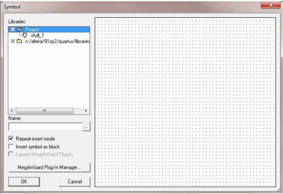
Figure 7-4
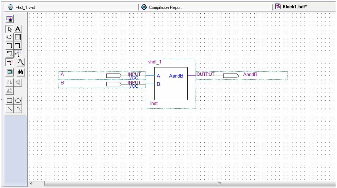
Figure 7-5
- Before compiling this bdf file, we need to name this bdf file and save it as part of our project under your subfolder. Choose File > Save As and enter File name as lab7_1. Place a check mark in the space labeled Add file to current project and press Save.
- Compile the project by selecting Processing > Start Compilation, or press Ctrl-L, or use the Compilation button in the toolbar. The compilation takes several seconds. When it is complete it should give a message that indicates, “Full compilation was successful”. Press OK. If unsuccessful, correct all errors and try to re-compile.
Simulating a Vector Waveform File (vwf)
- As you have done step 23 through 28 in the Part 1 of Lab6, you need to create a Vector Waveform File (vwf) to simulate a design(bdf) file. Add all inputs and output, specify an end time of 16 µs and a grid size of 1µs for our waveform display, and then save it as lab7_1.vwf.
- Select Processing – Start Simulation, or press Ctrl-I, or use the Simulation button in the toolbar. After a few moments a message stating “Simulation was successful” should appear. Click OK.
- The Simulation Waveforms appear in the Simulation Report shown in the Figure 7-6. You may have to expand the size of the Simulation Waveforms to suit your need and choose View > Fit in Window to see the entire 16µs waveform.
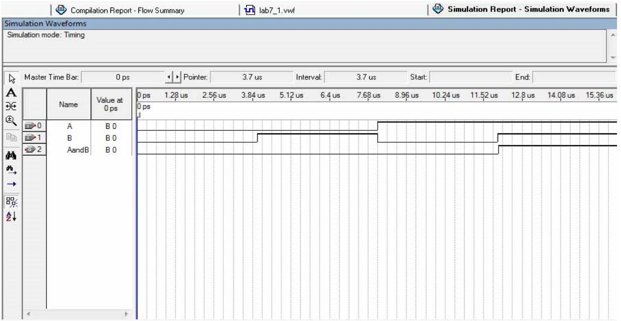
Figure 7-6
-
Compare the simulation result with that of the lab6_1.vwf.
Part 2 Altera DE2 Board
Altera’s DE2 Development and Education Boards has been developed to provide an ideal vehicle for learning about digital logic and computer organization in a laboratory setting. It uses the state-of-the-art technology in both hardware and CAD tools to expose students to a wide range of topics covered in typical courses. The power of the board is such that it is also highly suitable for a variety of design projects as well as for the development of sophisticated digital systems. In addition to the DE2 board and the associated software, Altera provides supporting materials that include tutorials, laboratory exercises, and interesting demonstrations.
DE2 Board

Figure 7-7 Altera’s DE2 Development and Education Board (By BreakdownDiode (Own work) [CC BY-SA 3.0], via Wikimedia Commons)
Connecting the Computer to the FPGA Board
To design and implement circuits on the DE2 board, it is necessary to follow the steps below.
- Plug the supplied 9 volt DC power supply into an AC power outlet (100V-240V), and then connect this power supply to the DE2 board. Make sure the RUN/PROG switch is in the RUN position.
-
Connect the DE2 board to your computer using the supplied USB cable (USB blaster cable port is located in the right next to the power cable on the board). And turn on the DE2 power by pressing the red power button on the board (see Figure 7-7). You should be able to observe the followings:
- The blue POWER LED is on and the blue GOOD LED ( Cyclone II FPGA configured) is on
- The 7-segment displays show a sequence of characters
- The red and green LEDs are flashing
- The LCD display shows Welcome to the Altera DE2 Board
Assigning Pin Numbers in the lab7_1.bdf file
- Now, we will assign specific pin numbers and recompile the lab7_1.bdf file before programming the Cyclone II FPGA. Choose Assignment > Pin Planner (Figure 7-8) and assign the pin numbers for inputs and outputs under the Location column. The Quartus II Compiler was free to choose any pins on the selected FPGA to serve as inputs and outputs. However, the DE2 board has hardwired connections between the FPGA pins and the other components on the board. We will use two toggle switches, labeled SW1 and SW0, to provide the external inputs, A and B, to our example circuit. We will connect the output, AandB to the green light-emitting diode labeled LEDG0 (see Table 7-1). When you assign the pin numbers, you can type number in the blank and press Enter or double-click it and select the pin number under the Location column (See Figure 7-9). If you want to use other toggle switches and LEDs, please see the DE2 User Manual for other pin assignments.
| Name | Component | Pin Location | |
| Input | A | SW1 | PIN_N25 |
| Input | B | SW0 | PIN_N26 |
| Output | AandB | LEDG0 | PIN_AE22 |
Table 7-1 Pin Assignment
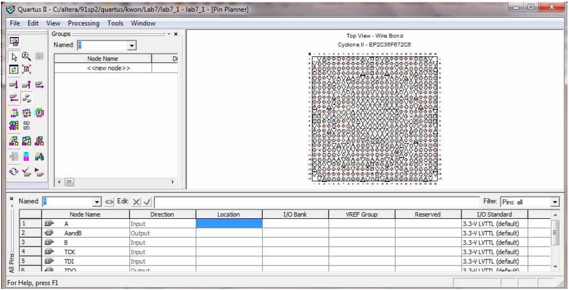
Figure 7-8
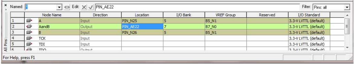
Figure 7-9
- To save the pin assignments as part of the project, choose File > Save Project. You can also simply close the Pin Planner window. If you go back to the lab7_1.bdf file, the circuit diagram will now have the pin assignments listed next to each input and output pin as shown in Figure 7-10.
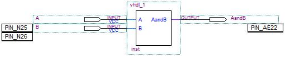
Figure 7-10
- The project must now be recompiled to synthesize the circuit with the specified pin assignments. Choose Processing > Start Compilation. (Press Yes if it asks to Save Changes to File.) After the compilation is successful press OK.
Programming and Configuring the DE2 board
The FPGA device must be programmed and configured to implement the designed circuit. The required configuration file is generated by the Quartus II Compiler’s Assembler module. Altera’s DE-series board allows the configuration to be done in two different ways, known as JTAG and AS modes. The configuration data is transferred from the host computer (which runs the Quartus II software) to the board by means of a cable that connects a USB port on the host computer to the leftmost USB connector on the board. To use this connection, it is necessary to have the USB-Blaster driver installed. If this driver is not already installed, consult the tutorial Getting Started with Altera’s DE-Series Boards for information about installing the driver. Before using the board, make sure that the USB cable is properly connected and turn on the power supply switch on the board.
In the JTAG mode, the configuration data is loaded directly into the FPGA device. The acronym JTAG stands for Joint Test Action Group. This group defined a simple way for testing digital circuits and loading data into them, which became an IEEE standard. If the FPGA is configured in this manner, it will retain its configuration as long as the power remains turned on. The configuration information is lost when the power is turned off. The JTAG mode is made by selecting the RUN position on the RUN/PROG switch of the DE2 board. For our convenience, we keep using the JTAG mode.
-
Select Tools > Programmer to reach the window in Figure 7-11. Here it is necessary to specify the programming hardware and the mode that should be used. If not already chosen by default, select JTAG in the Mode box. Also, if the USB-Blaster is not chosen by default, press the Hardware Setup… button and select the USB-Blaster in the window that pops up, as shown in Figure 7-12.
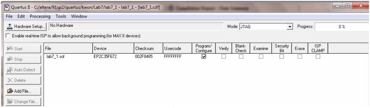
Figure 7-11
-
Observe that the configuration file lab7_1.sof is listed in the window in Figure 7-11. If the file is not already listed, then click Add File and select it. This is a binary file produced by the Compiler’s Assembler module, which contains the data needed to configure the FPGA device. The extension .sof stands for SRAM Object File. Note also that the device selected is EP2C35F672, which is the FPGA device used on the DE2 board. Click on the Program/Configure check box, as shown in Figure 7-11.
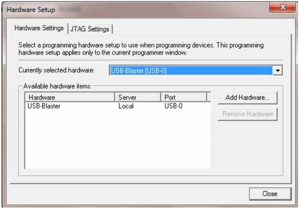
Figure 7-12
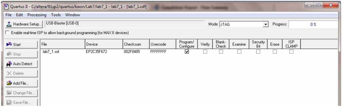
Figure 7-13
-
Now, press Start in the window in Figure 7-13. An LED on the board will light up when the configuration data has been downloaded successfully. If you see an error reported by Quartus II software indicating that programming failed, then check to ensure that the board is properly powered on.
Testing the Designed Circuit on the DE2 Board
-
Having downloaded the configuration data into the FPGA device, you can now test the implemented circuit. Flip the RUN/PROG switch to RUN position. Try all four valuations of the input variables A and B, by setting the corresponding states of the switches SW1 and SW0, respectfully. Verify that the circuit implements the truth table in Lab 6 or simulation results in Figure 7-6. The connections from the switches and LED to the DE2 board will allow you to test its logic operation. Remember, Each LED is driven directly by a pin on the Cyclone II FPGA; driving its associated pin to a high logic level turns the LED on, and driving the pin low turns it off.
| A (SW1) | B(SW0) | X (LEDG0) |
| 0 (DOWN) | 0 (DOWN) | 0 (OFF) |
| 0 (DOWN) | 1 (UP) | 0 (OFF) |
| 1 (UP) | 0 (DOWN) | 0 (OFF) |
| 1 (UP) | 1 (UP) | 1 (ON) |
Table 7-2 Truth table for Testing the DE2 board
Part 3 Practice
- Use Quartus II software to design the Boolean equation
.
- Design a VHDL File (vhdl file) for X.
- Create a Block Design File (bdf file) for X using the symbol created from the vhdl file.
- Create a Vector Waveform File (vwf) for X. The simulation should show all possible combination of inputs.
- Compare the result of the vector waveform with that of Lab6.
- Program a bdf file for X into DE2 Board and show the output to your instructor. Before showing it, you need to build the truth table for testing the DE2 board in Table 7-3 and complete the Table 7-4 for the pin assignments.
- Include the copies of vhdl and bdf files and vwf file in the lab report.
| A | B | C | X |
| 0 | 0 | 0 | |
| 0 | 0 | 1 | |
| 0 | 1 | 0 | |
| 0 | 1 | 1 | |
| 1 | 0 | 0 | |
| 1 | 0 | 1 | |
| 1 | 1 | 0 | |
| 1 | 1 | 1 |
Table 7-3 Truth table for testing DE2 board
| Inputs | Output |
| A: Pin _________
B: Pin _________ C: Pin _________ |
X: Pin _________ Pin ____ |
Table 7-3 Pin assignments