Contents
Equipment/Parts Needed
- Digital Trainer (Logic Probe)
- Breadboard
- 7400 NAND gate
- 7402 NOR gate
- 7404 Inverter
- 7408 AND gate
- 7432 OR gate
Objective
- The universality of the NAND and NOR gates means that they can be used as an inverter and the combinations of NAND/NOR gates can be used to implement the AND, OR, and all other logic operations.
- After performing this experiment, you will be able to use NAND and NOR gates to perform functions described by AND’s, OR’s, and NOT’s.
Discussion
-
The NAND gate is a universal gate because it can be used to produce the NOT operation, the AND operation, the OR operation, and the NOR operation. An inverter can be made from a NAND gate by connecting all of the inputs together and creating, a single input as shown below.
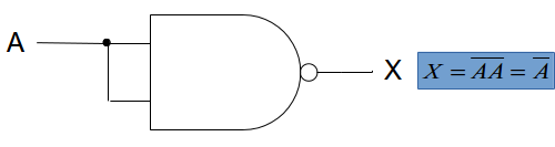
Figure 5-1 An inverter operation generated by the use of NAND gate
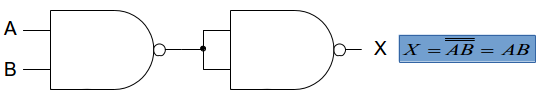
Figure 5-2 An AND operation generated by the use of two NAND gates
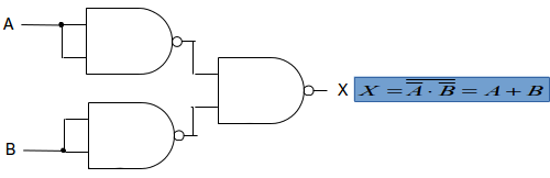
Figure 5-3 An OR operation generated by the use of three NAND gates
-
A Truth Table defines how a combination of gates will react to all possible input combinations.
-
A Logic Probe is a piece of test equipment which displays the logic level at a point in the circuit. 0 to 0.8V = Logic 0 and lights the L indicator. 2.0V to 5.0V = Logic 1 and lights the H indicator. Invalid logic voltage levels light neither indicator.
Part 1
1) Find the Boolean equation for the logic circuit shown in Figure 5-4.
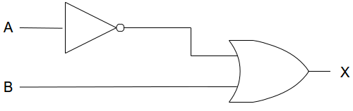
Figure 5-4 Logic Circuit for part 1 .
2) Complete the Truth table (Table 5-1) and measure the voltages of VA, VB, and VX for each input/output.
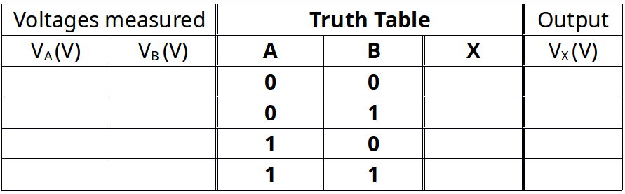
Table 5-1 Truth table and volts measured for input/output for Figure 5-4
3) Reconstruct the circuit above using only NAND gates. Include Boolean algebra, truth tables, and logic diagrams for the circuit reconstructed with only NAND gates.
3-1) Boolean algebra expression
3-2) Draw the reconstructed circuit and logic diagram here (only NAND gates)
3-3) Built the truth table for the reconstructed circuit and measured the voltage for each input/output
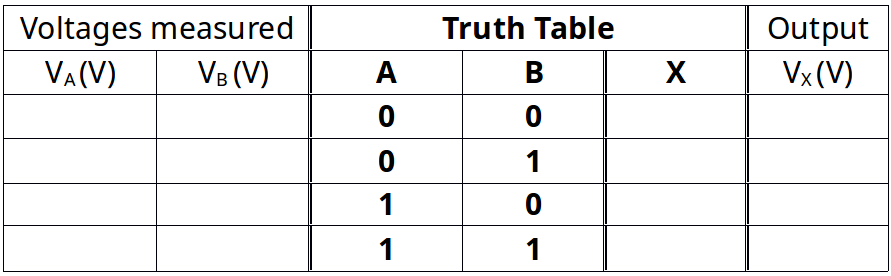
Table 5-2 Truth table and volts measured for input/output for the reconstructed circuit
Part 2
1) Find the Boolean equation for the logic circuit shown in Figure 5-5.

Figure 5-5 Logic Circuit for part 2.
2) Complete the Truth table (Table 5-3) and measure the voltages of VA, VB, VC, and VY for each input/output
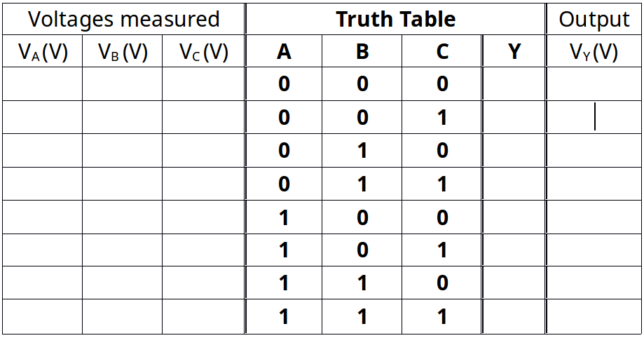
Table 5-3 Truth table and volts measured for input/output for Figure 5-5.
3) Then reconstruct the circuit above using only NOR gates. Include Boolean algebra, truth tables, and logic diagrams for the circuit reconstructed with only NOR gates.
3-1) Boolean algebra expression
3-2) Draw the reconstructed circuit and logic diagram here (only NOR gates)
3-3) Built the truth table for the reconstructed circuit and measured the voltage for each input/output
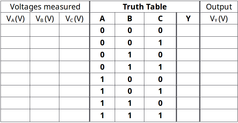
Table 5-4 Truth table and volts measured for input/output for the reconstructed circuit.
Questions/Report
- Why are NAND gates and NOR gates sometimes referred to as universal gates?
- Why would a designer want to form an AND gate from two NAND gates?
- Using only four NAND gates, draw the logic circuit for NOR gate.
- How many inverters could be formed using a 7400 NAND IC?