Contents
Equipment/Parts Needed
- PC (Altera Quartus II V9.1 installed)
- DE-2 board
Objective
- Design a half adder by extracting the Boolean equation from a truth table.
- Design a full adder by extracting the Boolean equation from a truth table.
- Construct the half adder and full adder circuits from a Boolean equation.
- Design and test a 3-bit adder circuit with using the Quartus II development software with the DE-2 board.
Discussion
The fundamental building block of addition is the half adder, whose truth table is shown in the Table 10-1. By observation, you may recognize that the Carry output is the AND gate with respect to inputs A and B. The Sum output is the exclusive OR gate with respect to inputs A and B.
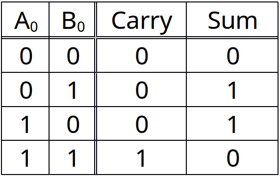
Table 10-1 Half adder truth table
The full adder is a circuit with the three inputs, A, B, CIN, and two outputs, Sum and Carry. The truth table for the full adder is shown in the Table 10-2.
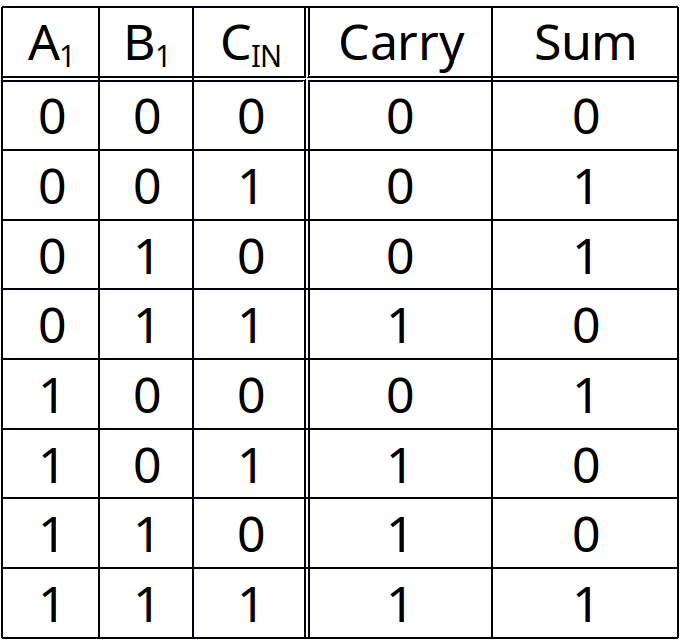
Table 10-2 Full adder truth table
Part 1: Half adder circuit
- Open the Quartus II software. Select File – New Project Wizard. Enter the appropriate drive letter for the designated storage area on the computer you are using followed by the working directory C:\altera\91sp2\quartus\kwon\Lab10. You need to go through the step from 1 through 8 in the Part 1 of Lab6 manual. Don’t forget to create the folder Lab10 under the subfolder of your last name. Assign the project name Lab10_1, assign Cyclone II for the device family, and select the EP2C35F672C6 chip in the Family & device settings [page of 3 of 5].
- Create the Boolean equation from the truth table that represents the Carry output with respect to inputs A0 and B0.
Carry = _____________________________________
- Write the Boolean equation from the truth table that represents the Sum output with respect to inputs A0 and B0.
Sum = ______________________________________
- Open a new Block diagram/Schematic file (File > New) and construct the circuits of a half adder based on your equations. Each symbol should be available in the Project Library in the Symbol diagonal box.
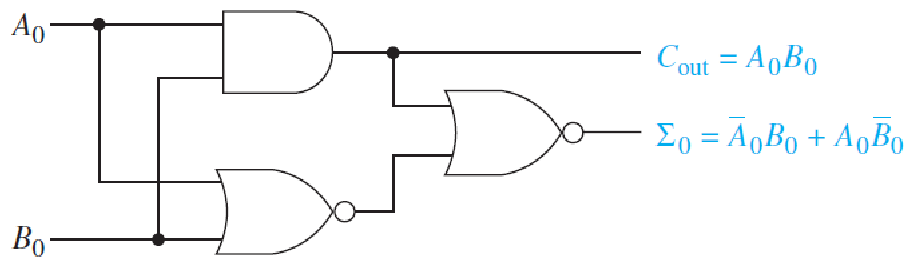
Figure 10-1 Half adder circuit
- Before compiling this bdf file, we need to name this bdf file and save it as part of our project under your subfolder. Choose File > Save As and enter File name as lab10_1. Place a check mark in the space labeled Add file to current project and press Save.
- Compile the project by selecting Processing > Start Compilation, or press Ctrl-L, or use the Compilation button in the toolbar. The compilation takes several seconds. When it is complete it should give a message that indicates, “Full compilation was successful”. Press OK. If unsuccessful, correct all errors and try to re-compile.
- You need to create a Vector Waveform File (vwf) to simulate a design(bdf) file. Add all inputs and output, specify an end time of 1 µs and a grid size of 100ns for our waveform display, and then save it as lab10_1.vwf.
- Select Processing – Start Simulation, or press Ctrl-I, or use the Simulation button in the toolbar. After a few moments a message stating “Simulation was successful” should appear. Click OK.
- The Simulation Waveforms appear in the Simulation Report. You may have to expand the size of the Simulation Waveforms to suit your need and choose View > Fit in Window to see the entire waveform.
Part 2: Full adder circuit
- Create the Boolean equation from the truth table that represents the Carry output with respect to inputs A1 and B1.
Carry = _____________________________________
- Write the Boolean equation from the truth table that represents the Sum output with respect to inputs A1 and B1.
Sum = ______________________________________
- Create the project Lab10_2, assign Cyclone II for the device family, and select the EP2C35F672C6 chip in the Family & device settings [page of 3 of 5]. Do not select a different project directory, click NO.
- Open a new Block diagram/Schematic file (File > New) and construct the circuits of a full adder based on your equations.
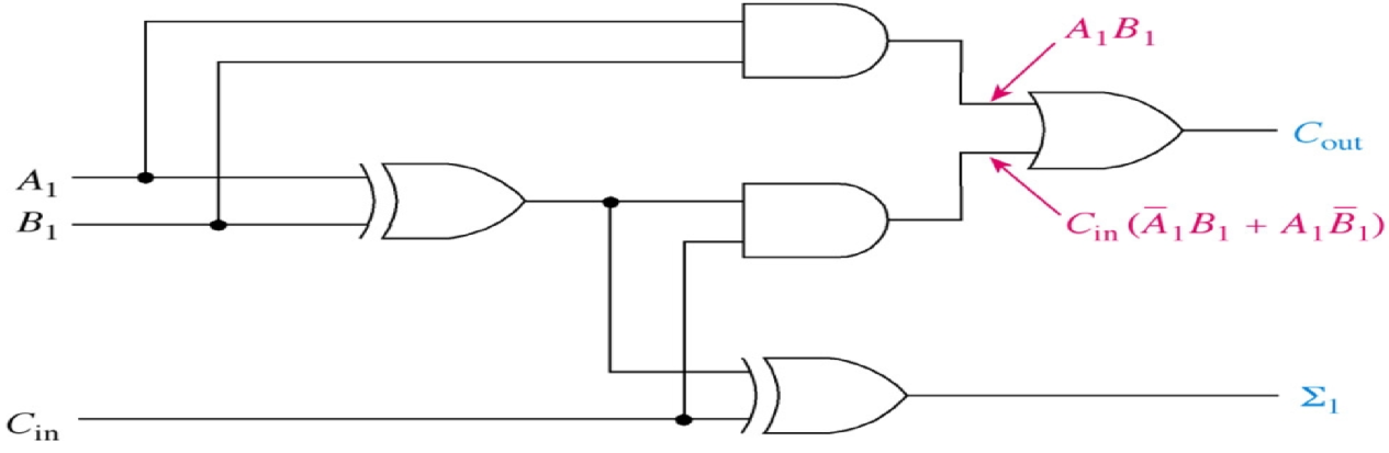
Figure 10-2 Full adder circuit
- Before compiling this bdf file, we need to name this bdf file and save it as part of our project under your subfolder. Choose File > Save As and enter File name as lab10_2. Place a check mark in the space labeled Add file to current project and press Save.
- Compile the project by selecting Processing > Start Compilation, or press Ctrl-L, or use the Compilation button in the toolbar. The compilation takes several seconds. When it is complete it should give a message that indicates, “Full compilation was successful”. Press OK. If unsuccessful, correct all errors and try to re-compile.
- Create a Vector Waveform File (vwf) to simulate a design (bdf) file. Add all inputs and output, specify an end time of 1 µs and a grid size of 100ns for our waveform display, and then save it as lab10_2.vwf.
- Select Processing – Start Simulation, or press Ctrl-I, or use the Simulation button in the toolbar. After a few moments a message stating “Simulation was successful” should appear. Click OK.
- The Simulation Waveforms appear in the Simulation Report. You may have to expand the size of the Simulation Waveforms to suit your need and choose View > Fit in Window to see the entire waveform.
Part 3: 3-bit Full adder circuit
- Fill in the truth table with the expected outputs of a 3-bit Adder circuit.
-
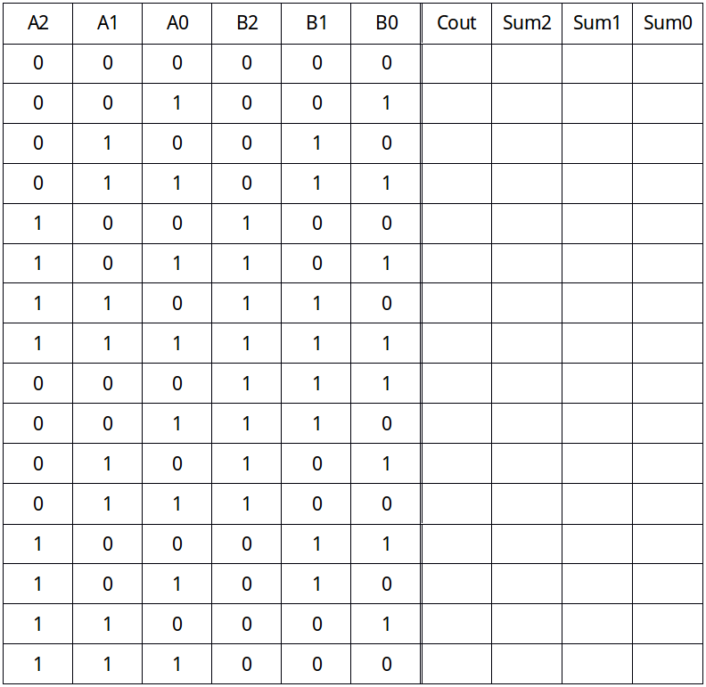
Table 10-3 3-bit Full adder truth table
Start the Quartus II software. Select File – New Project Wizard. And create a new project name under the directory C:\altera\91sp2\quartus\your last name\Lab10. Assign the project name Lab10_3, assign Cyclone II for the device family, and select the EP2C35F672C6 chip in the Family & device settings.
- Open a New Block Diagram/Schematic file and draw the circuit for 3-bit binary adders shown in Figure 10-3. And compile the circuit and correct all errors if you have any.
-
- Open a new Vector Waveform file and create waveforms all inputs (A0 through B2). And simulate the waveforms and analyze the output waveforms with respect to the inputs, and then compare the outputs with your Truth table.
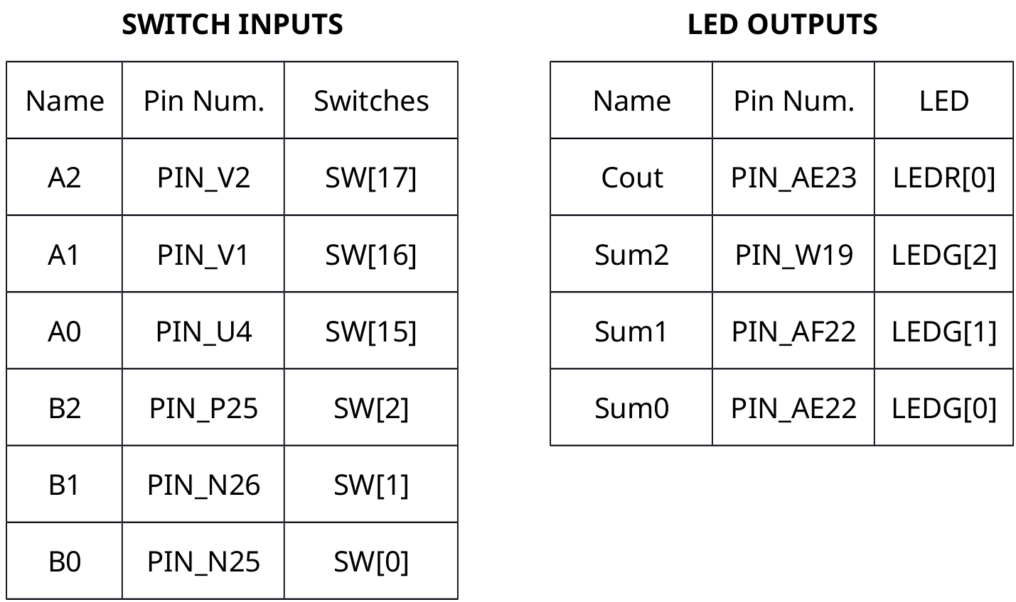
- To program files and test it on DE-2 board, choose Assignment > Pins and then assign the pin numbers as shown in the tables below.
- Save and compile the design again before programming. Then connect DE-2 board to computer. (If you’re not sure, refer to the Part 2 of Lab 7 manual.)
- Now program the design and exercise the toggle switches and verify the proper LED is illuminated by comparing with the truth table in Table 10-3 where you filled with above. You need to show and explain it to your Instructor. (Remember that Input switches in the ON position mean a HIGH(1). Also remember that the DE-2 board has active-HIGH LEDs.)
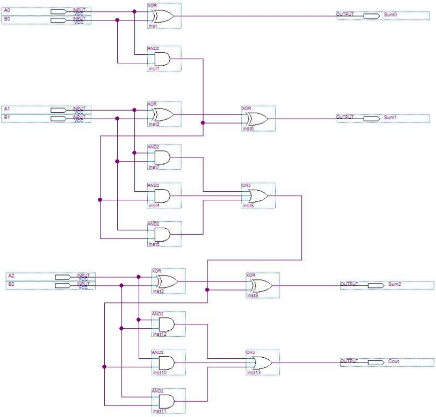
Figure 10-3 3-bit Binary Adder Circuit
Questions/Report
- Include the schematics, vector waveforms, truth tables, and pin outs in the lab report.
- What is the range of values for an 8-bit unsigned binary number?