Contents
Equipment/Parts Needed
- Quartus IIR Web Edition V9.1 SP2 software by Altera Corporation
- USB drive to save your files
Objective
- Learn how to use the Quartus IIR V9.1 SP2 software to create a schematic, create waveforms, compile, and simulate a circuit
- Analyze waveforms and develop truth tables for logic circuits
Discussion
The Tools toolbar icons you will be using in this lab are identified in Figure 6-1. These icons are located at the top of the Quartus II application window. This horizontal toolbar contains buttons such as: New, Open, Save, Print, Cut, Copy, Paste, Undo and Redo. Other toolbar buttons will be discussed in the lab where appropriate.

Figure 6-1
Part 1 Quartus II Tutorial
Open the Quartus II
- From the desktop, select Start – Programs – Quartus II. This lab is based on the Web Edition.
If your computer is connected to the Internet, Quartus II automatically checks for updates and displays a message in the work area should updates exist on the altera.com website. Once the software opens, you will see a menu bar at the top of the screen with names similar to those you would find in most Windows-based programs, that is, File, Edit, View, Tools, Window, and Help. See Figure 6-2. Various Utility windows appear below the toolbar depending on which ones have been selected (View – Utility Windows). The size of each window may be changed by placing the mouse on the border. When the mouse pointer changes to two lines, click and hold the left mouse button down as you move the mouse (click and drag) in the direction desired to reduce or increase the size of these windows. You may also click the corresponding close button to eliminate the window, hence increasing the size of the work area.
Creating a New Project
- From the main menu, select File > New Project Wizard. See Figure 6-3. An Introduction box may appear describing the features of the New Project Wizard. Click Next.
- Page 1 of 5 of the New Project Wizard appears (See Figure 6-4). Enter the Working directory, project name and name of your top-level entity of your project. Examples shown in this lab manual will show drive C. Enter the appropriate drive letter for your designated storage area on the computer you are using or select the directory with Browse (…) followed by the working directory C:\altera\91sp2\quartus\kwon\Lab6. (I recommend that you create a subfolder of your last name such as ‘kwon’ as shown above so that you always keep and save your files under your subfolder) Enter lab6_1 as the project name and as the top-level entity name. By default, the top-level entity name and project name will be the same; however, you may enter a different top-level entity name.

Figure 6-2

Figure 6-3
- If the directory name does not exist, a Warning box will appear stating such as [“Directory c:\altera\91sp2\quartus\kwon\Lab6” does not exist. Do you want to create it?]. Click Yes. Directories that do not exist will be created by the software when Yes is clicked.

Figure 6-4
- Page 2 of 5 of the New Project Wizard allows you to select design files, software source files and non-default libraries. Since you are just getting started, none of these exist so just click Next.
- Page 3 of 5 of the New Project Wizard (Figure 6-5) allows one to select the device family. This screen will allow us to specify the actual CPLD that we will target for our design. In the dropdown box for the Family, select Cyclone II. Place a check in the box for Specific device. Highlight the EP2C35F672C6 and click Next.

Figure 6-5
- Page 4 of 5 of the New Project Wizard allows one to specify Electronic Design Automation (EDA) tools to be used with this project. Since this project does not use any of the third party tools listed, make sure None is specified as the Tool Name for each Tool Type. Click Next.
- Page 5 of 5 of the New Project Wizard (Figure 6-6) displays a summary of your selections. Review the choices and either click Back to correct an entry or click Finish to create the project. The top-level design entity name appears in the Hierarchy tab of the Project Navigator window and the title of the project will be displayed in the Title bar of the Quartus II window.

Figure 6-6
Creating a Block Design File (bdf)
- To draw the logic circuit for our Boolean equation (X=AB), we will use the block editor to create a Block Design file by drawing the schematic. Open a new Schematic file (File > New) by highlighting Block Diagram/Schematic File. And click OK.
- Before drawing the logic circuit we need to name this bdf file and save it as part of our project under your subfolder. Choose File > Save As and enter File name as lab6_1. Place a check mark in the space labeled Add file to current project and press Save (Figure 6-7).

Figure 6-7
- A column of icons appears to the left of the Block Diagram window. These icons are identified in Figure 6-8 and will be referenced to by name as the lab progresses.
- Now you are ready to enter the logic symbol. Click the Symbol Tool icon. A Symbol dialog box will appear with the library file C:/quartus/libraries shown in the Libraries Window. Click on the box with a plus sign to open that directory. Open subdirectories primitives and logic and select the and2 symbol. (See Figure 6-9.)

Figure 6-8

Figure 6-9
- De-select the Repeat-insert mode then click OK. Position the symbol near the center of the Block Diagram window then click the left mouse button to anchor the symbol in place. The Repeat-insert mode box by default is checked, allowing for multiple gates to be inserted into the schematic file. If left checked, right click the mouse button and select Cancel after inserting your first symbol into the schematic file.
- Hint: If you know the name of the symbol, you can type the symbol name in the Name window without the need to search the directories for that symbol.
- Available libraries are the Altera primitives containing basic logic building blocks, macrofunctions (mf) of the 7400 family logic (available in the others directory), and megafunctions containing library of parameterized modules (LPMs) for high-level circuit functions. Browse the subdirectories to become acquainted with the symbols available for your use.
- Add two input and one output pin to your schematic. Input and output symbols are available in the C:/altera/91sp2/quartus/libraries/primitive/pin directory. Position these symbols as shown in Figure 6-10.

Figure 6-10
- To reposition a symbol, single click on the left side of that symbol to “click and drag” the symbol to the desired position.
- To change the name “PIN_NAME” of the input (or output) connector, double-click on the current name. When the name appears in reverse text (highlighted), type the new name. Change the current names of the input connectors to A and B and change the output connector’s name to X. Your circuit should now look like the circuit in Figure 6-11.

Figure 6-11
- Add lines from each gate terminal to the respective input or output terminal. To make these lines, position the mouse pointer on a gate terminal. When the mouse pointer turns into a cross, click and drag the mouse so that it barely touches the input or output connector lead. Do not drag and release the wire inside a component. The circuit should appear as shown in Figure 6-12.

Figure 6-12
- To save the updated bdf file, choose File > Save.
Compiling the Project
- Now we will compile the project. In this step Quartus II performs an analysis and synthesis of the bdf file to make sure that there are no errors in our logic. It then fits the design to a template of an EP2C35F672C6. Finally, it runs an assembler and timing analyzer. To run the compiler, choose Processing / Start Compilation.
- The compilation takes several seconds. When it is complete it should give a message that indicates, “Full compilation was successful”. Press OK.
Creating a Vector Waveform File (vwf) to simulate the Design
- Now that the circuit is constructed, you are ready to create a set of input waveforms. Select File > New, then highlight Vector Waveform File then click OK. The Waveform1.vwf Vector Waveform file will appear on the screen.
- Before drawing the simulation waveforms we need to name this vwf file and save it as port of our project under your subfolder. Choose File > Save As and enter a file name of lab6_1 (same as your bdf file name). Place a check mark in the space labeled Add file to current project and press Save.
- To build this simulation file we first need to specify an end time of 16 µs and a grid size of 1µs for our waveform display:
- Choose Edit > End time > 16 in time > µs, then click OK.
- Choose Edit > Grid Size > Period > 1 > µs, then click OK.
- To see the entire 16µs display, choose View > Fit In Window.
Adding the inputs and Outputs to the Waveform (vwf) Display
- To add the inputs and outputs that we want to simulate on the waveform display, place your mouse pointer in the first field below the Name column, then double-click the left mouse button. The Insert Node or Bus dialog box will appear. Select Node Finder (Figure 6-13). Under “Filter” select “Pins: all” then select “List.” Drag all input/ouput nodes with the left mouse button and hit the button (>) to copy all the nodes (inputs and outputs) to the “Selected Nodes” list on the right. Select OK. Select OK again.

Figure 6-13
- You should now see the inputs and outputs in the vector waveform file window. Save this file again. The window should look like in Figure 6-14.

Figure 6-14
- In order to test all of the possible combinations for our two inputs we need to create a series of timing waveforms that step through all 4 possible combinations of input logic levels. The easiest way to do this is to form a binary counter that count from 0000 up to 0100 just like we did with a truth table. In the vwf file screen, left click on the first input A, choose Value > Clock, and then Enter a period of 16µs and click OK. To draw the B waveform as a clock with a period of 8µs, choose Value > Clock, and then Enter a period of 8µs and click OK. Then save it again. When completed, the vwf screen should look like Figure 6-15.

Figure 6-15
Performing a Simulation of the Output
- To perform a simulation, choose Processing > Start Simulation. After a few moments a message stating “Simulation was successful” should appear. Click OK.
- The Simulation Waveforms appear in the Simulation Report shown in the Figure 6-16. You may have to expand the size of the Simulation Waveforms to suit your need and choose View > Fit in Window to see the entire 16µs waveform.

Figure 6-16
If you haven’t created a logic table for the equation you entered under Quartus, do so now and compare these results with those obtained from simulation. The table that actually is needed is a voltage table, but since all the signals were assumed active-high for this example, they will look identical (with 0 and 1 replaced with L and H, respectively). Your simulation results from Quartus should match your logic table.
Printing the Simulation Results
- To print a waveform file, select “File > Print.” If you want to print only a portion of the waveform, select “File > Print > Options” and select the “Time range” as desired. A poor alternative to the above is to capture a portion of the screen and to then paste this captured portion into a word processing or drawing application. To copy a simulation output (or any window on the screen), make it as big as possible and then (while it is the active [selected]), hit “Alt-Print Scrn” (i.e., hold down the “Alt” and while still holding it, press the “Print Scrn” key). Then paste the captured window into your favorite word-processing or drawing program. In your chosen program you can crop and enlarge you figure as desired.
Functional Compilation and Simulation
- When designing something big, it is a good idea to keep a lot of data available for simulation. Then, when you know that your design simulates correctly, you can remove as many outputs as needed to get the design to fit into your particular device. Extra signals can be output and used in your simulation. I call these extra outputs debug outputs. A functional compilation and simulation has (effectively) no limit on the number of inputs, outputs and internal elements available. Below, I discuss how to functionally compile and simulate your design in Quartus. First design your parts as usual (either with the graphics editor or in VHDL). There is no need to assign a device to the design.
- To compile functionally, pull up the “Compiler Tool.” This tool can be found under “Processing | Compiler Tool.” Select the left-most button under “Analysis and Synthesis.” (This button has an triangle point right, an AND gate, and a check mark.) This will compile your design without trying to fit it into any particular part. When your design compiles without error, you are ready to functionally simulate.
- Create a waveform file as you have done previously. Open the “Simulator Tool” under Processing | Simulator Tool.” Under “Simulation Mode” select “Functional.” Then select the button labeled “Generate Functional Simulation Netlist.” Check the box labeled “Overwrite simulation input file with simulation results.” Select the “Start” button. Your functional simulation will now be completed. The functional simulation will not show propagation delays. Compare this simulation output to the timing simulation output done previously (with propagation delays).
Part 2 Practice
-
-
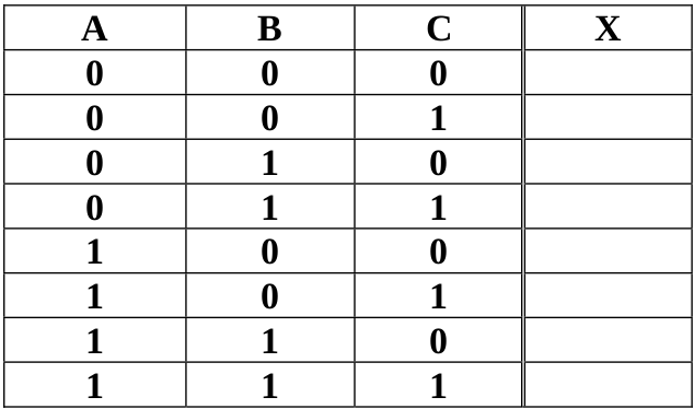
- Use Quartus II software to design the Boolean equation Y=AB+C .
- Build the truth table for X.
- Design the Block Design File (bdf file) for X.
- Create a Vector Waveform File (vwf) for X. The simulation should show all possible combination of inputs.
- Compare the result of the vector waveform with the truth table.
- Include the copies of bdf file and vwf file in the lab report.
- Use Quartus II software to design the Boolean equation Y=AB+C .
-
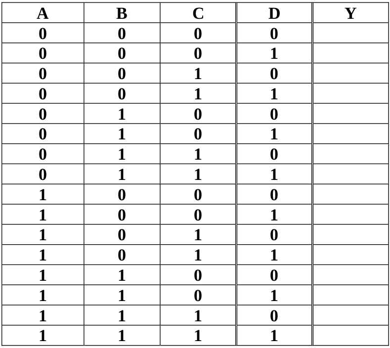
- Use Quartus II software to design the Boolean equation Y=AB+CD .
- Build the truth table for X.
- Design the schematic (bdf file) for Y.
- Create a Vector Waveform File (vwf) for Y. The simulation shows all possible combination of inputs.
- Compare the result of the vector waveform with the truth table.
- Include the copies of schematic file and vector waveform file in the lab report.