Contents
Equipment/Parts Needed
- Quartus IIR Web Edition V9.1 SP2 software by Altera Corporation
- USB drive to save your files
Objective
- Use simple VHDL assignment statements to represent a function table
- Introduce the selected signal assignment WHEN-ELSE clause
- Display hexadecimal numbers (0 through F) on the 7-segment LED of the DE-2 board
Discussion
Seven segment LED displays are often found in clock radios, VCRs, microwave ovens, toys and many other household items. They are primarily used to display decimal numbers but they can also display a few alphabets and other characters. This experiment describes interfacing a seven segment LED display to the DE-board. You will display a hexadecimal value from 0 (00h) to 15 (0Fh) on the seven segment LED display.
A seven segment LED display is a special arrangement of 7 LED elements to form a rectangular shape using two vertical segments on each side with one horizontal segment on the top, middle, and bottom. By individually turning the segments on or off, numbers from 0 to 9 and some letters can be displayed. Seven segment displays sometime also have an eighth segment to display the decimal point. Therefore, a seven-segment display will require seven outputs from the schematic design to display a number, and one more output if the decimal point is to be displayed too. (This experiment ignores the decimal point.)
The 7 LEDs inside the display can be arranged with a common cathode or common anode configuration. With a common cathode display, the cathodes of all the segment LEDs are tied together and this common point must be connected to the ground. A required LED segment is then turned on by applying a logic 1 to its anode. In common anode displays, all the anodes are tied together and the common anode is connected to the supply voltage Vcc. Individual segments are turned on by applying logic 0 to their cathodes. Since D2-2 has a common anode 7-segment, displaying a number requires turning on and off the proper segment LEDs. For example, to display a number 7, only segments a, b, and c should be turned on, which means their logic levels should be low.
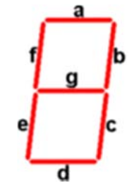
Figure 8-1 7-segment LED
Let’s assign a bus value using D3,D2, D1, and D0 to represent each bit position in a 4-bit bus, D[3…0]. Also, the outputs will be represented by a 7-bit bus, S[6..0], which will be assigned ‘g’, ‘f’, ‘e’, ‘d’, ‘c’, ‘b’, and ‘a’ for the 7-segment, respectively, as shown in Table 8-1.
Assuming the buses are properly defined in the Entity Declaration, we can say that bus S will take on the 7-bit value that corresponds to the value of bus D.
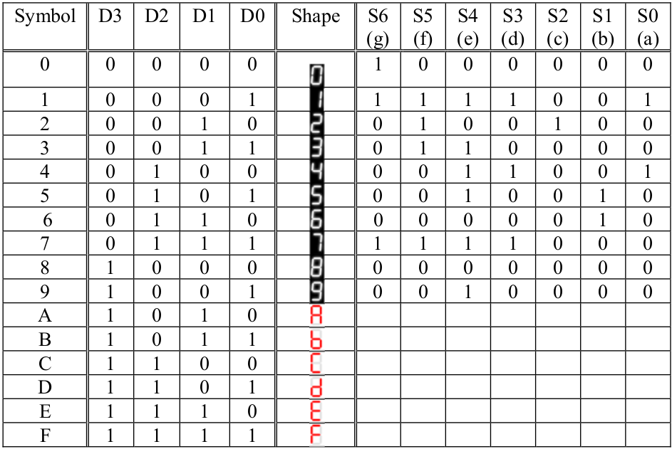
Table 8-1
Text Box 8-1
Part 1 Procedure
Creating a New Project
- Open the Quartus II software. Select File – New Project Wizard. Enter the appropriate drive letter for the designated storage area on the computer you are using followed by the working directory C:\altera\91sp2\quartus\kwon\Lab8. You need to go through the step from 1 through 8 in the Part 1 of Lab7 manual. Don’t forget to create the folder Lab8 under the subfolder of your last name. Assign the project name Lab8_1, assign Cyclone II for the device family, and select the EP2C35F672C6 chip in the Family & device settings [page of 3 of 5].
Creating a VHDL File (bdf)
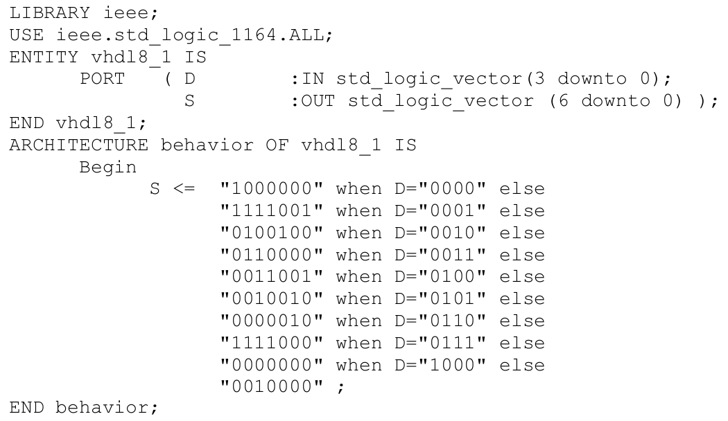
- Open a new VHDL Device Design file (File > New) by highlighting VHDL File. Type the VHDL codes shown in Text Box 8-1.
- Save the VHDL file as vhdl8_1.vhd as part of our project under your subfolder. Place a check mark in the space labeled Add file to current project and press Save.
- Select File > Create/Update > Create Symbol Files for Current File to create a symbol file for the VHDL code entered. A display window should soon appear stating that the Create Symbol File was (or not) successful. Click OK and close the Compilation Report window.
- Open a new Schematic file (File > New) by highlighting Block Diagram/Schematic File. And click OK. And construct the circuit shown in Figure 8-2 using the symbols you just created. Each symbol should be available in the Project Library in the Symbol diagonal box.
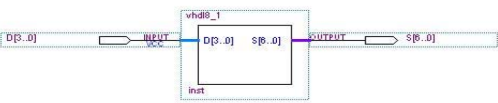
Figure 8-2
- Before compiling this bdf file, we need to name this bdf file and save it as part of our project under your subfolder. Choose File > Save As and enter File name as lab8_1. Place a check mark in the space labeled Add file to current project and press Save.
- Compile the project by selecting Processing > Start Compilation, or press Ctrl-L, or use the Compilation button in the toolbar. The compilation takes several seconds. When it is complete it should give a message that indicates, “Full compilation was successful”. Press OK. If unsuccessful, correct all errors and try to re-compile.
Simulating a Vector Waveform File (vwf)
- As you have done step 23 through 28 in the Part 1 of Lab1, you need to create a Vector Waveform File (vwf) to simulate a design(bdf) file. Add all inputs and output, specify an end time of 1 µs and a grid size of 1ns for our waveform display, and then save it as lab8_1.vwf.
- When creating the D[3..0] bus, enter D for the bus name, select Hexadecimal for the Radix, and enter 4 for the Bus Width in the Node Properties window. When created, the D waveform will appear with a plus sign implying that it can be ungrouped to show the individual bits, D[3], D[2], D[1], and D[0].
-
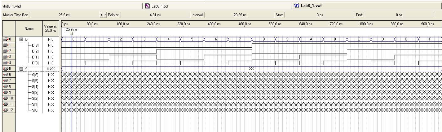
Figure 8-3
Select Processing – Start Simulation, or press Ctrl-I, or use the Simulation button in the toolbar. After a few moments a message stating “Simulation was successful” should appear. Click OK.
- The Simulation Waveforms appear in the Simulation Report. You may have to expand the size of the Simulation Waveforms to suit your need and choose View > Fit in Window to see the entire waveform.
Connecting the Computer to the FPGA Board
To design and implement circuits on the DE2 board, it is necessary to follow the steps below.
- Plug the supplied 9 volt DC power supply into an AC power outlet (100V-240V), and then connect this power supply to the DE2 board. Make sure the RUN/PROG switch is in the RUN position.
-
Connect the DE2 board to your computer using the supplied USB cable (USB blaster cable port is located in the right next to the power cable on the board). And turn on the DE2 power by pressing the red power button on the board. You should be able to observe the followings:
-
- The blue POWER LED is on and the blue GOOD LED ( Cyclone II FPGA configured) is on
- The 7-segment displays show a sequence of characters
- The red and green LEDs are flashing
- The LCD display shows Welcome to the Altera DE2 Board
Assigning Pin Numbers in the lab8_1.bdf file
-
Now, we will assign specific pin numbers and recompile the lab8_1.bdf file before programming the Cyclone II FPGA. Choose Assignment > Pin Planner and assign the pin numbers for inputs and outputs under the Location column. The Quartus II Compiler was free to choose any pins on the selected FPGA to serve as inputs and outputs. However, the DE2 board has hardwired connections between the FPGA pins and the other components on the board. We will use four toggle switches, labeled SW3 through SW0, to provide the external inputs, D3 through D0. We will connect the output, a 7-segment labeled HEX0 (see Table 8-2). When you assign the pin numbers, you can type number in the blank and press Enter or double-click it and select the pin number under the Location column. If you want to use other toggle switches and LEDs, please see the DE2 User Manual for other pin assignments.
- Program your schematic design into DE-2 board to display the values from ‘0’ through ‘9’.
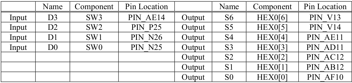
Table 8-2 Pin Assignment
-
To save the pin assignments as part of the project, choose File > Save Project. You can also simply close the Pin Planner window. If you go back to the lab8_1.bdf file, the circuit diagram will now have the pin assignments listed next to each input and output pin.
- The project must now be recompiled to synthesize the circuit with the specified pin assignments. Choose Processing > Start Compilation. (Press Yes if it asks to Save Changes to File.) After the compilation is successful press OK.
Programming and Configuring the DE2 board
-
Select Tools > Programmer to reach the window in Figure 8-4. Here it is necessary to specify the programming hardware and the mode that should be used. If not already chosen by default, select JTAG in the Mode box. Also, if the USB-Blaster is not chosen by default, press the Hardware Setup… button and select the USB-Blaster in the window that pops up.
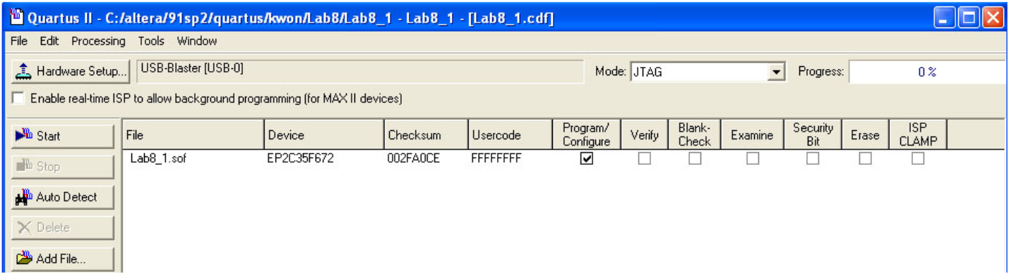
Figure 8-4
-
Observe that the configuration file lab8_1.sof is listed in the window in Figure 8-4. If the file is not already listed, then click Add File and select it. This is a binary file produced by the Compiler’s Assembler module, which contains the data needed to configure the FPGA device. The extension .sof stands for SRAM Object File. Note also that the device selected is EP2C35F672, which is the FPGA device used on the DE2 board. Click on the Program/Configure check box, as shown in Figure 8-4.
- Now, press Start in the window in Figure 8-4. An LED on the board will light up when the configuration data has been downloaded successfully. If you see an error reported by Quartus II software indicating that programming failed, then check to ensure that the board is properly powered on.
Testing the Designed Circuit on the DE2 Board
- Having downloaded the configuration data into the FPGA device, you can now test the implemented circuit. You can display the number from ‘0’ through ‘9’ on the 7-segment using the toggle switches SW3 through SW0.
Part 2 Practice
- Complete the Table 8-1 and display the value from 0 through F on the 7-segment of DE-2 board.
- Create the VHDL codes for the values from ‘A’ through ‘F’ (which means to add the VHDL codes for ‘A’ through ‘F’ in the Table 8-1.).
- Create a Block Design File (bdf file) for the output using the symbol created from the vhdl file.
- Create a Vector Waveform File (vwf) for the output . The simulation should show all possible combination of inputs.
- Include the copies of vhdl codes and bdf file and vwf file as well as your pin assignment in the lab report.