
Contents
Equipment/Parts Needed
- 5V DC Power Supply
- Digital Trainer (Logic Probe)
- Breadboard
- DIP Switch
- 7404 (Inverter)
- 7408 (AND gate)
- 7432 (OR gate)
- Digital MultiMeter
Objective
- To exam a logic circuit and investigate the operation of the NOT, OR and AND Gates.
- To verify logic truth tables from the voltages measured.
Discussion
- NOT, OR and AND gates are the basic logic gates. All other logic functions can be derived from these three.
- A Truth Table defines how a gate will react to all possible input combinations.
- A Logic Probe is a piece of test equipment which displays the logic level at a point in the circuit. 0 to 0.8V = Logic 0 and lights the L indicator. 2.0V to 5.0V = Logic 1 and lights the H indicator. Invalid logic voltage levels light neither indicator.
Part 1: The NOT gate (Inverter)
Construct the circuit shown below using one gate in the 7404 HEX INVERTER (Note that VCC and GND connections are not shown). Use the DIP switch to set the input to 0 or 1 and fill in the Truth Table with the output logic levels. Use the Logic Probe to
determine logic levels.
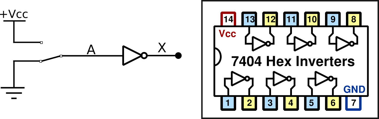
Figure 2-1 The Circuit for NOT gate and 7404 pinout diagram

Table 2-1 Truth table for Figure 2-1
Part 2: The OR gate
Construct the circuit shown below using one gate in the 7432 QUAD OR GATE (Note that VCC and GND connections are not shown). Use two sections of the DIP switch to set the inputs to 0 or 1 and fill in the Truth Table with the output logic levels. Use the Logic Probe to determine logic levels.
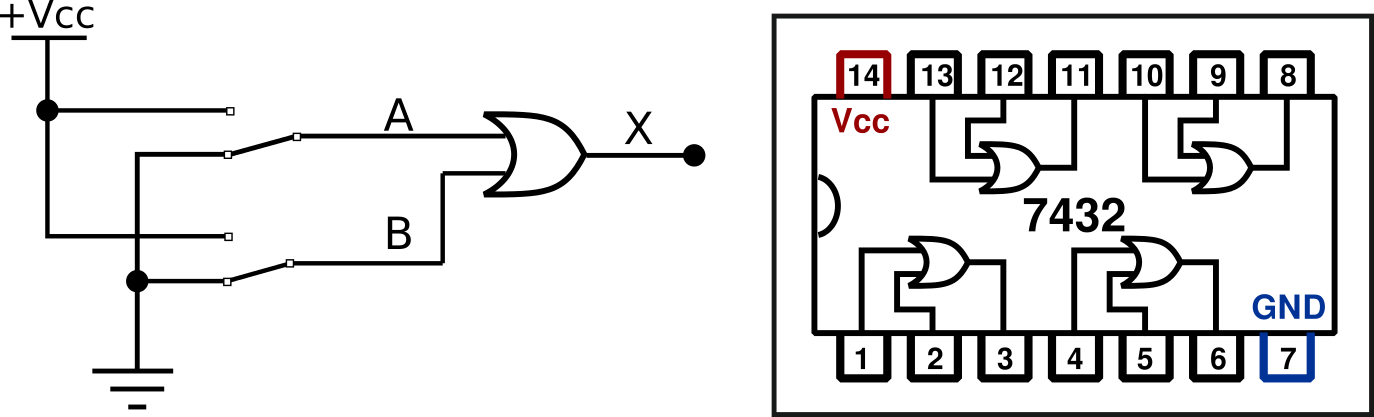
Figure 2-2 The circuit for OR gate and 7432 pinout diagram

Table 2-2 Truth table for Figure 2-2
Part 3: The AND gate
Construct the circuit shown below using one gate in the 7408 QUAD AND GATE (Note that VCC and GND connections are not shown). Use two sections of the DIP switch to set the inputs to 0 or 1 and fill in the Truth Table with the output logic levels. Use the Logic Probe to determine logic levels.
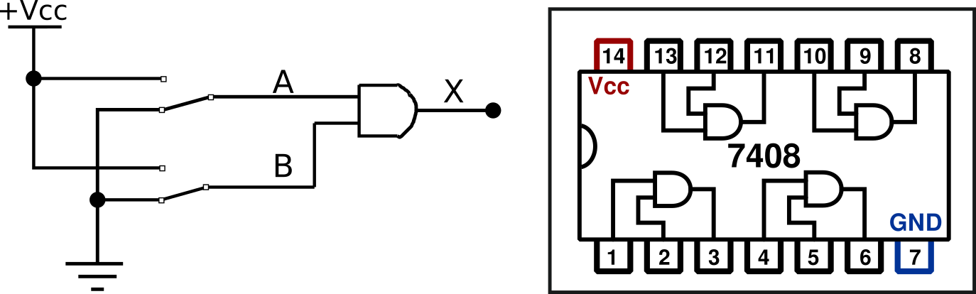
Figure 2-3 The circuit for AND gate and 7408 pinout diagram
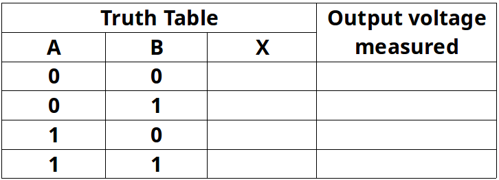
Table 2-3 Truth table for Figure 2-3
Questions/Report
- What are the Boolean expressions for the NOT, OR and AND gates?
- Under what input conditions is the output of a 2 input OR gate LOW? Under what input conditions is the output of a 2 input AND gate HIGH?
- We are given a 3 input AND gate and want to use it as a 2 input AND gate. Two inputs to the AND gate are connected to the two input signals. How would you connect the third gate input?
- If one input to a 3 input OR gate were accidentally connected to VCC (shorted to VCC), how would the output of the OR gate react no matter what the other 2 input levels might be?
- If one input to a 3 input AND gate were accidentally connected to Ground (shorted to Ground), how would the output of the AND gate react no matter what the other 2 input levels might be?