Objective: dissect the POE Network Switch and its power supply, examine the inner parts, trying to understand how they work, then put everything back together; dissect small Chinese electronic device, examine inner parts, then put them back together, trying to vivisect the device.
Materials: Cisco/Linksys SRW 2008 MP 8-port Gigabit switch, AC/DC power supply, Chinese electronic device, screwdrivers (Phillips and flat-head), hex wrenches, camera, vise grips, Craftsman insulated pry bar, safety glasses.
Procedure:
- Identify inputs and outputs of the network switch:
– 8 Gigabit ports inputs;
– 1 Serial port output;
– 2 Mini-GBIC connectors outputs;
– 1 48vDC 3.1A power input;
2. Examine AC/DC power supply;
3. Use the flat-head screwdriver to remove the rubber feet;
4. Use Phillips screwdriver to remove the screws out of the bottom of the power supply;
5. Because the power supply is not designed to be dissected easily, its bottom screws are very long and made from a soft metal. When unable to remove stripped screws, switch to the pry bar (use safety glasses);
6. After opening the power supply, examine its inner parts:
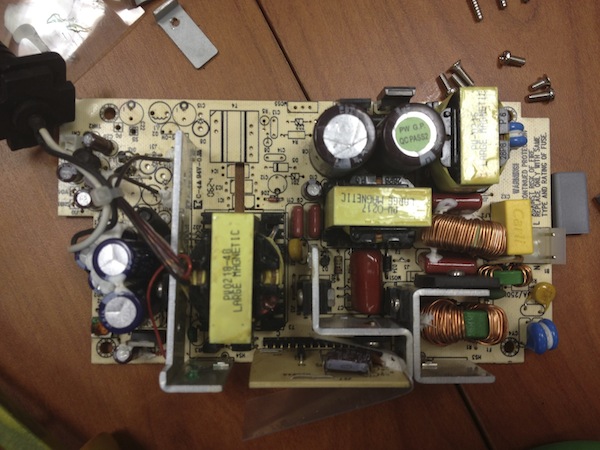
 There are a lot of electrolytic and ceramic capacitors of different sizes, as well as resistors, heat sinks, metal coils and other components. The most interesting thing is the PCB itself, because it was made using an “old school” thru-hole method, meaning that an real person was putting all the components into the holes of the PCB and then was soldering everything manually. Also, there are some empty slots for the components on the PCB. It is because the PCBs are mass produced and their configuration varies from one device to another. When some additional components are needed, the manufacturer just inserts them into the pre-made empty slots, instead of making a different PCB. The second interesting thing was green paint on some of the inner screws. When removing these screws, the paint would be immediately stripped off them, indicating that someone was touching them and voiding warranty of the device;
7. Examine Cisco/Linksys Network Switch. There are some mounting holes on the sides;
8. Pop the case apart by using a flat-head screwdriver;
9. Pop off the front bezel panel: there is a little ribbon connector going to the PCB;
10. Remove the screws holding the PCB to the case;
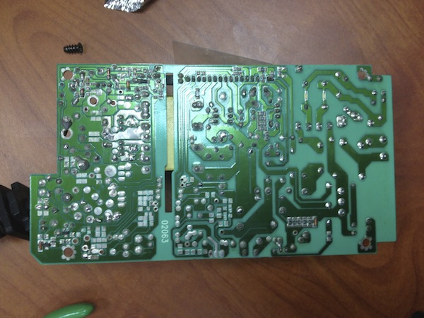
11. Examine the PCB:
 This PCB is much more sophisticated than the power supply’s one. It uses а very complex circuit with a lot of integrated chips. Unlike the previous PCB (made using a thru-hole method) this board is made using surface-mount technology (meaning that all components are mounted directly into the surface of the PCB, without drilling holes). Because SMT is fully automated and very precise technology, the components of the Linksys PCB are much smaller than those of the power supply’s board;
12. Remove the daughter board from the PCB, using a hex wrench (to get rid of the hex standoff screws);
13. Examine the daughter board:
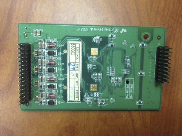 Like the mother board, this PCB is also made using SMT. There are two sets of the PCB mount connectors on the back of the daughter board.
Results:
We were able to put apart the power supply and the Cisco/Linksys network switch. The overall procedure was successful, but very time consuming; as a result, we didn’t have time to put everything together and move on to the next device.