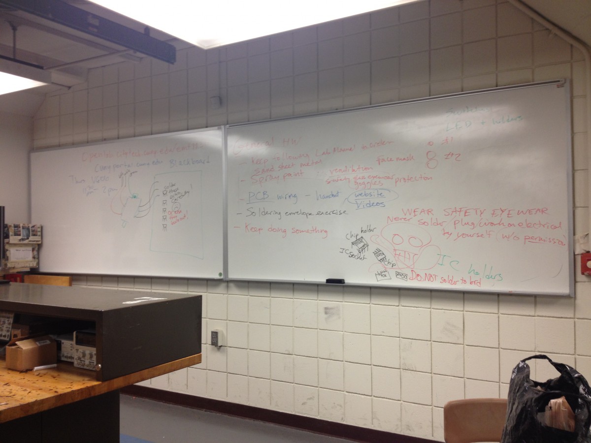
EMT1130 Mon 11/2/15 notes
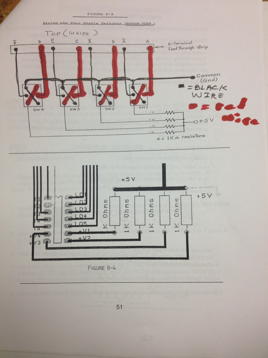
Urgent last Wiring diagram for signal connections
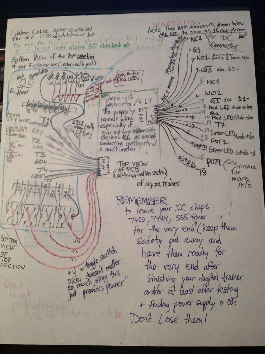
EMT1130 Mon 10/26/15 notes
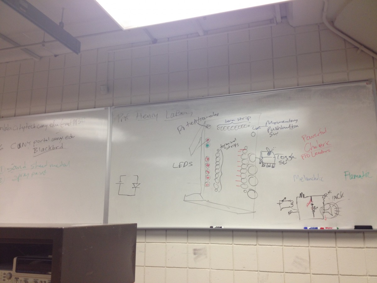
Toggle Switch wiring highlights
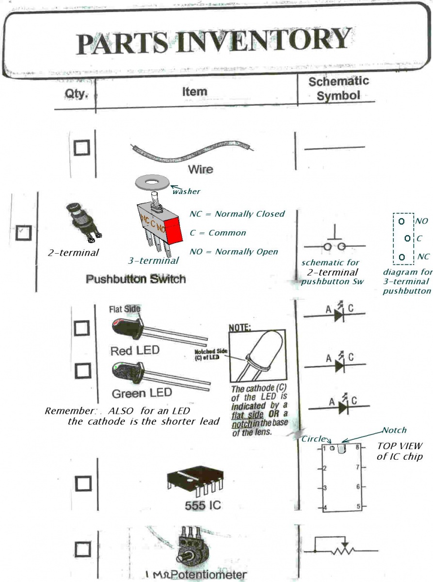
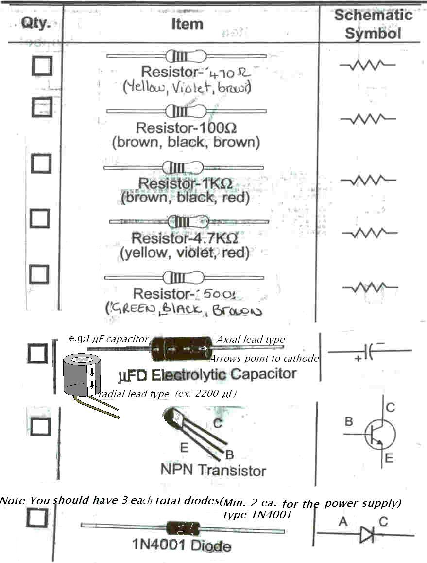
Please click to enlarge or view larger version of the files attached/uploaded to this site (this will show you different important parts/electrical and/or electronic components to be used in the EMT1130 digital trainer you are constructing)
This is a default assignments page. I enter some assignments like the EMT1130Procedure here, but may delete this page if I don’t wish to use it (for example the activity called “Class PCB manufacturing Process” is NOT REQUIRED OFFICIALLY UNLESS OTHERWISE STATED BY YOUR INSTRUCTOR).
Please see the following (as extra useful planning assignment – may serve for research ideas outside of main regular class duties/requirements – but please do not sacrifice your course progress just to explore the software explain below!!! ALWAYS STICK TO THE MAIN ASSIGNMENTS AS SPECIFIED BY YOUR INSTRUCTOR USING THE EMT1130 LAB MANUAL FOR ULTIMATE REFERENCE AND ASK INSTRUCTOR AND CLASS LAB TECHNICIAN FOR HELP ON ANYTHING UNCLEAR):
Printed Circuit manufacturing Process
Materials Required
PCB CAD Software . This Software is available as free download from PAD2PAD.
Go to the http://pad2pad.com/ and locate the software and download to your computer. For instruction in how to use the software see the video training. Click to this link for this video training.
http://www.pad2pad.com/video/intro.htm Watch the full video to be familiar with the creation of PC boards. If you have any questions address to your instructor.
Procedure
1. – Click on the Pad2Pad Icon PCB CAD Software will open.
2. – Go file Select “New” Board Setting Windows will open.
3. – In the Board Setting follow the configuration as shown in the attached “Class PCB manufacturing Process” file (located elsewhere on this site).
4. – Answer OK to the Warning window.
5. – The Drawing window will appear. In Here you will start placing the parts according the Diagram of the electronic Design.
6. – Click the Footprint (Chip Symbol at the Right Toolbar) the following window will appear: “Footprints and Component Manager”
7. – Select PTH then Select Diodes and select 1N4007 and Placed on Board
8. – Place all the devices on the board listed on the diagram for the Power Supply listed on page 42 from your manual. Go to capacitors and place Radial capacitor Electrolyte. Place the transistor; go to “TO” “Semiconductor TO220” and Paced on the Board.
9. – Select the Trace Tool and Select 0.30” You can modify the size of the trace according to your needs and start connecting the parts in the board and wiring according to the Diagram.
10. – After you finished placing and wiring the Power Supply page 42 then you will continue with the other sections according to the Diagram. Pages 47, 50, 53, 55 and 57.
11.- In other to have the exact layout of the device you will look the Diagram and look for the parts by name in the software and placed on the Board, then wired using wire 0.30” for the + 5V line and 0.25” for the other connections.
You may obtain THE FINAL LAYOUT OF THE PCB from the “Class PCB manufacturing Process” MS Word file
NOTE: IC7400 Pin 14 would Need a Jump wire soldered to the +5V Line in order to work
FINAL VIEW OF EMT1130 PRINTED CIRCUIT BOARD is shown in the previously mentioned file prepared Prof. De La Cruz as of 2009.


Anyone willing to share some relevant ideas on printed circuit board (PCB) design, preparation, manufacturing processes ? For example, you may have noticed a piece of equipment which is from http://www.lpkf.com/